
![]()
![]()
Electronic and optic microscopes
Electron and optic microscopes
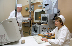
Electron microscope Zeiss SUPRA55VP
Super-high resolution field-emission scanning electron microscope Zeiss SUPRA55VP, Carl Zeiss AG, Germany, with energy-dispersive spectrometer Inca Energy 350, wave spectrometer Inca Wave 500 and HKL EBSD Premium System (Oxford Instruments, GB) for registration and analysis of backscatter electron diffraction.
Resolution: at 15kV – 10nm; at 1kV – 1.7nm, at 100V – 4.0nm; resolution of system HKL CHANNEL 5 (phase) - 25nm.
Low vacuum range: 1-133Pa, that allows working with non-conductive samples. Operation at low accelerating voltage (from 100V) allows examination of samples sensitive to irradiation and super-thin samples.
While energy-dispersive and wave spectrometer are traditional for the analytical scanning electron microscopy, microscopes equipped with HKL CHANNEL 5 for registration and analysis of backscatter electron diffraction are quite rare nowadays. This system allows indexation of phases both with high and low symmetry as well as analysis of materials with pseudosymmetry. The system is equipped with software to analyze texture of any crystalline material by the method of pole figures, reverse pole figures, distribution of orientations/disorientations in the Euler’s space, etc. The system has a wide range of crystallographic data.
This microscope is equipped with INCA Synergy, a system based on energy-dispersive analyzer Inca Energy and EBSD HKL Channel 5, for the simultaneous analysis of structure, texture and chemical composition. This system provides application of both backscatter electron diffraction and energy-dispersive X-ray micro-analysis to identify automatically phases and plot maps of phase distribution, crystallites orientations and X-ray maps of elements distribution.
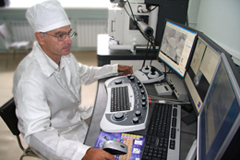
Electron microscope XL 30 ESEM-TMP
Scanning remote electron microscope XL 30 ESEM-TMP (Philips, Holland) with INCA AE 530 for micro-analysis (energy-dispersive and wave spectrometer). The microscope column and spectrometers are located in the hot cell. Resolution: at 30kV – 3.5nm, at 1kV – 25nm. The microscope is equipped with a system and a detector allowing examinations under low vacuum, including examinations of non-conductive samples.
Electron microscope JEM 2000 FXII
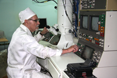
Transmission electron microscope JEM 2000 FXII (JEOL, Japan) equipped with GENESIS XM 2 System 60 TEM, EDAX, USA for X-ray microanalysis has a device for electron beam scanning, a detector of secondary and reflected electrons and a goniometer.
It allows:
- examination of the dislocation structure, radiation defects and surplus phase precipitates under transmission mode using specimens in the form of thin foils;
- investigation of material surface structure under scanning mode in the secondary and reflected electrons;
- quantitative and qualitative analysis of the matrix and precipitates particles in the transmission and scanning modes.
Thinned disks 3mm in diameter or specimens 8*3*1.5mm are used for examination.
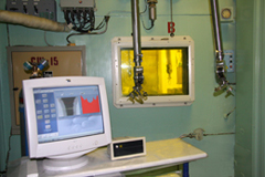
Microscope MIM15
Research metallographic remotely-controlled microscope MIM15 (“LOMO”, Russia) is intended for examination of micro-structure of irradiated materials. It provides visual examination and photographing of the metal structure in the light background, direct and inclined light, dark background and polarized light. The area to be examined is photographed at the required magnification (100, 200, 400, 600, 1000 dpi) and light.
All rights reserved. Use of the website materials is prohibited unless a link to the website is provided © 2008-2023
JSC “SSC RIAR”, Russian Federation, 433510, Ulyanovsk region, Dimitrovgrad, Zapadnoye Shosse, 9.
E-mail: niiar@niiar.ru. Tel.: +7 (84235) 9-83-83. Fax: +7 (84235) 9-83-84